
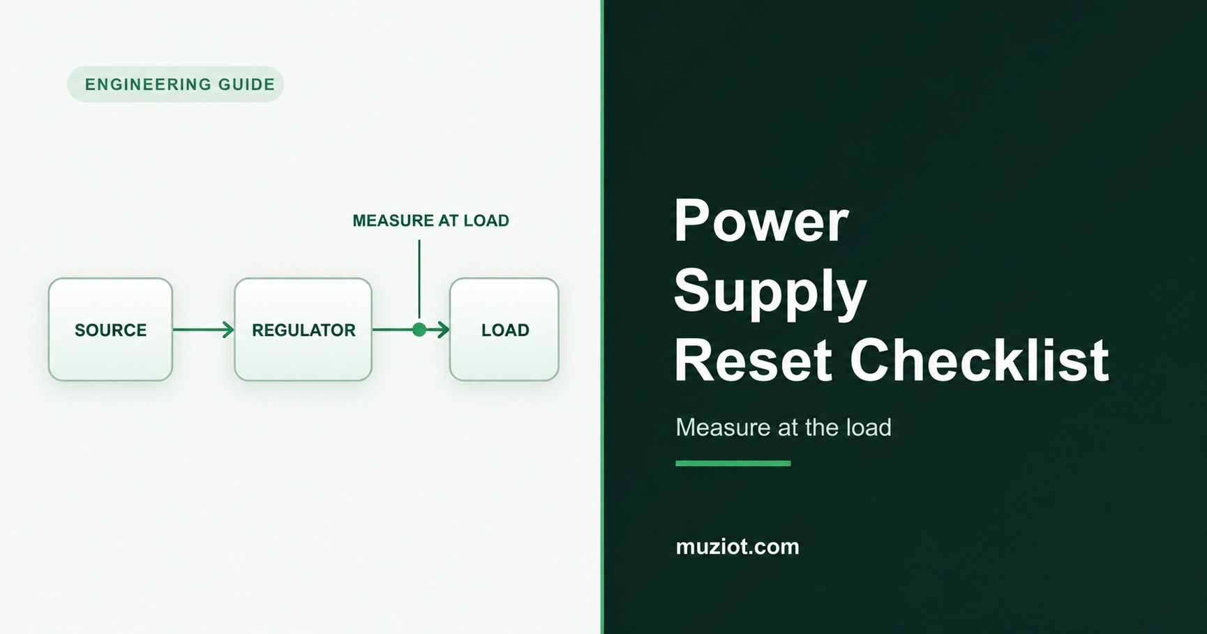
If a cellular modem disappears during an upload, first confirm whether the modem restarted. A USB disconnect, host reset, controlled shutdown or network registration failure can produce a similar log entry. Identify the event and the hardware's actual power input before changing capacitors.
This measurement checklist is for engineers integrating a bare cellular module or a Mini PCIe card into a host. The EC25-AF examples use public Quectel V2.4 manuals to distinguish two power inputs. Their electrical values apply to those document revisions. Before approving an actual design, match the full ordered part and hardware revision to the applicable hardware guide.
Identify the actual power input
Write down the full manufacturer part number, hardware revision, firmware, and hardware form: soldered module, Mini PCIe card, USB dongle or carrier board. Start the supply review at the input your host actually powers. If the module itself is still being selected, begin with the broader cellular module specifications and design guide.
Swipe the table to see all columns.
| Hardware form | Supply point to check | Documented EC25 example |
|---|---|---|
| EC25-AF bare LCC/LGA module | Module VBAT_RF and VBAT_BB pins, plus their ground return | Quectel's public EC25 Series Hardware Design V2.4 assigns VBAT_RF to pins 57/58 and VBAT_BB to pins 59/60. That revision specifies 3.3-4.3 V at the module supply. |
| EC25-AF Mini PCIe card | Card-edge VCC_3V3 and ground pins | Quectel's public EC25 Mini PCIe Hardware Design V2.4 assigns VCC_3V3 to pins 2/39/41/52 and specifies 3.0-3.6 V at the card input. |
| Carrier board or USB dongle | The assembly's documented external input | A bare-module or Mini PCIe rating does not specify a third-party board's power connector. Request the board schematic and revision. |
Bare-module VBAT_RF/VBAT_BB and card-edge VCC_3V3 are different input domains. Keep their limits separate. In the 28 September 2026 directory check, Quectel's EC25 module page listed Hardware Design V2.8, and its Mini PCIe page listed V2.7. Those controlled documents were not reviewed for this guide; the table cites public V2.4 text. For a live design, obtain the revision that governs the ordered part. Muziot's EC25 LCC integration page describes the bare-module form, while the EC25 series selection page helps screen regional suffixes and hardware forms.
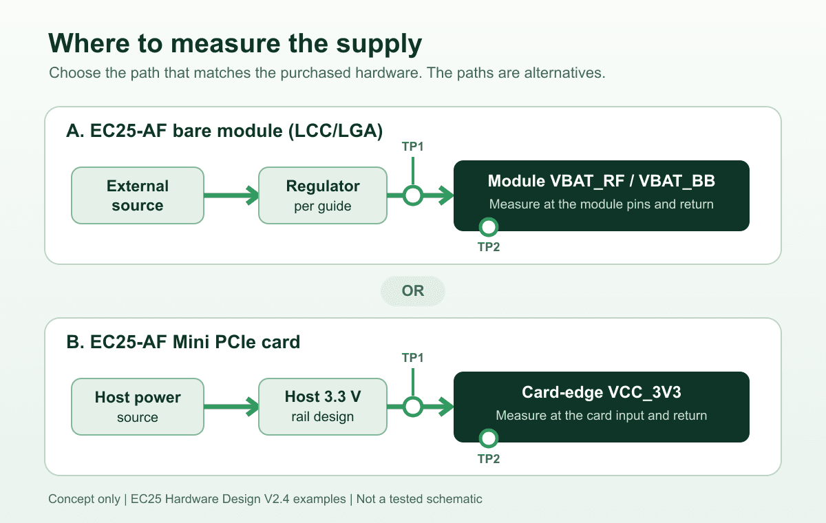
Figure 1. Conceptual measurement map. Choose the path that matches the purchased hardware. The bare-module and Mini PCIe paths are alternatives; this drawing is not a tested schematic.
Capture the failure before assigning a cause
Record what the host and modem do immediately before and after the event. Did the modem boot banner return, did only the USB device re-enumerate, or did the data session drop while the module remained responsive? Keep the host log, modem status, supply trace, and network event on a common time reference. A single "modem offline" message cannot distinguish these cases.
Start with a repeatable operation: power-on, registration, a sustained uplink, and the operation that users report as failing. Note the input source, cable or battery state, ambient conditions, antenna configuration, SIM, operator, firmware, and host software version. A weak radio path can change transmit activity, but a correlation between RF activity and a reset is not yet proof of a supply fault.
If another module or board revision appears stable, compare the complete power path and software state before calling the new part defective. The module replacement checklist covers the broader pin, RF, software, and compliance review.
Measure voltage at the load, not only at the regulator
Probe the regulator output and the actual module or card input during the same failing operation. On a bare EC25 design, the relevant load nodes are the VBAT supply paths and their nearby ground return. On a Mini PCIe design, start at VCC_3V3 on the card edge and the host connector ground. A healthy voltage at the regulator does not show what reaches the module after connectors, protection devices, traces, and cables.
Use a probing method appropriate to the expected transient. Keep the voltage-probe return short and record the probe arrangement. Account for measurement artifacts, especially when using multiple grounded oscilloscope channels; Texas Instruments explains how scope ground paths can distort dynamic-response readings. Capture the waveform, minimum observed voltage and event time. An average voltage or handheld meter reading cannot show whether a short transient meets the required limit.
Quectel's EC25 bare-module V2.4 guide says AT+CBC can monitor the VBAT_BB voltage value. That is a useful software observation, but it cannot replace a time-aligned measurement of a short event at the physical supply point. On other models, even the meaning of a reported voltage may differ: verify the relevant command manual.
Review the regulator, return path, and decoupling together
Read the current hardware guide for the exact module or card before choosing output voltage, transient current capability, bulk capacitance, and ceramic capacitors. The EC25 bare-module V2.4 guide shows one external source divided into RF and baseband paths, with local bypass components near the VBAT pins. Its reference values describe that guide's circuit. The EC25 Mini PCIe V2.4 guide describes a different 3.3 V card-input reference circuit and discusses a 2G transmit case. Neither circuit is a universal LTE-module bill of materials, and the 2G example is not a measured U.S. LTE result for EC25-AF.
Then check the actual host design:
- Can the source and regulator support the documented load step across the allowed input, temperature, and tolerance range? Check the regulator's transient behavior and current-limit response, not only its steady-state nameplate rating.
- Where are the bulk and high-frequency bypass parts relative to the load? Include capacitor tolerance, DC-bias behavior, ESR, placement, and the return path in the review. Increasing one capacitance value without examining the loop may leave the underlying drop unchanged.
- Does the input path include a long cable, narrow trace, switch, fuse, connector, or protection part whose drop increases under load? Compare regulator-output and load-input waveforms to localize the loss.
- Does the RF layout and switching-supply placement follow the module guide? Treat RF interference and supply integrity as separate checks even when both affect a connection.
These are inspection points, not a claim that any particular change fixes a specific board. If a revised layout or component value is proposed, review stability with the regulator vendor's data and verify it on the actual assembly.
Check power control and shutdown sequence
Supply voltage is only one way to stop a module. Record PWRKEY, RESET_N, any host power-enable signal, and USB state alongside the rail. A host brownout may toggle an enable pin even when the modem rail itself remains in range; software may also request a shutdown. Follow the exact module or card guide for pin polarity, sequencing, and recovery.
For the bare EC25 family, the public Hardware Design V2.4 guide describes normal shutdown through PWRKEY or an AT-controlled procedure before supply removal. Use the procedure and timing in the applicable guide. Sleep or idle current figures in a module datasheet describe specified module conditions; a gateway, tracker or battery system needs its own power budget.
Validate the design under the intended network load
After a proposed change, repeat the capture across the intended U.S. deployment conditions. Use the planned operator, SIM, bands, antenna, firmware and host revision. The Mini PCIe V2.4 manual's 2G transmit example does not establish an LTE acceptance limit for an EC25-AF deployment. Define the limits from the applicable document for the ordered part and the system's requirements.
Swipe the table to see all columns.
| Record for each run | What to capture |
|---|---|
| Identity | Complete module/card P/N, hardware and firmware revisions, host PCB revision, applicable manual revision. |
| Operating condition | Source voltage and type, temperature, operator/SIM, antenna, registration state, uplink operation, host software. |
| Electrical trace | Regulator output and physical module/card input, probe setup, minimum voltage, event time; current trace if safely available. |
| Behavior | Boot/USB/network logs, PWRKEY/RESET_N/enable state, repeat count, pass or fail against the agreed limit. |
Use this table to record project measurements. This guide contains no board waveforms or repair outcomes. The hardware team should review the actual board data and applicable manufacturer documents before signing off a design.
What to send for a documentation review
Include the full part number and requested hardware form, destination operator, host-board revision, power schematic, regulator part number and any available traces in a documentation request. State whether you need a bare module, Mini PCIe card or separate board assembly. These details support a discussion of module documents and the quoted configuration. Board validation and design approval remain with the customer's hardware team. Browse the Datasheet Center or send your module and board details with your BOM enquiry.
Engineering references
- Quectel EC25 Series Hardware Design V2.4, released 24 January 2022: the cited bare-module pin and power information, especially section 3.6.
- Quectel EC25 Mini PCIe Hardware Design V2.4, released 18 December 2019: the cited card-edge power supply information, especially sections 3.5 and 6.2.
- Texas Instruments, Measure Output Dynamic Response on Power Supplies: Oscilloscope Ground Issues: limits of dynamic rail measurements with grounded scope connections.